Optically Variable Devices (OVDs) – a revolution in anti-counterfeiting technology
In 1995 CSIRO’s Exelgram technology was voted by the Australian Academy of Technological Sciences and Engineering (ATSE) as one of Australia’s 100 greatest inventions of the 20th century. This nomination was in recognition of Exelgram’s reputation as the world’s most sophisticated anti-counterfeiting device. In 1997, after stiff competition from European and American security printing companies, Exelgram was incorporated into four denominations of US dollar-denominated American Express Travellers Cheques. After a year of circulation it was shown that Exelgram had reduced the counterfeiting rate of Amex cheques by 90%. Following this excellent result the International Hologram Manufacturers Association (IHMA) awarded CSIRO its excellence certificate for the Exelgram devices carried on these cheques. Later in 1998 American Express chose Exelgram technology again for the remainder of its US cheque denominations – thus reducing the counterfeiting rate to zero.
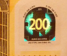
In the same year the company also chose Exelgram to protect its new Euro denominated travellers cheques. When first issued in January 1999 these Amex travellers cheques became the first Euro denomination financial transaction documents. Later Amex chose Exelgram to also protect its new series of Canadian currency cheques. Note that at the time Amex were selling US$26 billion of traveller’s cheques annually. Prior to these Amex projects Exelgram was adopted for use by Hungarian and Estonian banknotes, Ukrainian visas, Vietnamese bank cheques, security seals for King and Royal Cabinet of Saudi Arabia as well as various other projects. Exelgram applications are not limited to polymer substrates as in all of the above applications the Exelgram foils were applied to the paper document substrates. To this day the CSIRO Exelgram patents continue to be licensed to major European suppliers of banknote security products.
How it all started
CSIRO’s interest in optically variable devices (OVD) – flat film devices containing images which change form according to the viewing angle – had its genesis in the early 1970’s as part of what was then called the Currency Note Research and Development (CNRD) project. It was this project, located at the CSIRO Division of Applied Organic Chemistry, that led to the development of the Polymer banknote technology see Polymer banknotes. The original intention of this project was to develop OVD technology that could be incorporated into a banknote substrate. Polymer was chosen for this substrate because it was thought at the time that the surface roughness of paper banknote substrates would cause too much image degradation. This was a mistake as can be seen from the fact that today the vast majority of the world’s OVD banknotes use paper substrates.
Although no effective OVD was developed during the CNRD years which ended when the technology package was handed over to the Reserve Bank of Australia in 1980, significant progress was made in developing the mathematical and optical physics basis for the complex optical microstructures required for such a diffractive device. This work was later de-classified and published in a series of six papers in the Journal Optica Acta in 1983/1984. It was this mathematical optical physics theory that was to form the basis for the future development of CSIRO’s Catpix and Pixelgram OVD technologies.
Catpix I
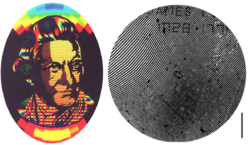
One of the key problems that needed to be overcome in developing a suitable OVD for banknotes was the image degradation problem associated with flexing and crumpling of the banknote during normal day-to-day financial transactions. This problem was overcome by the development of a specialised OVD optical microstructure which produced wavefronts that were structurally stable with respect to small crinkling perturbations of the OVD surface. These structurally stable optical wavefronts were members of a class of special functions known as diffraction catastrophes. The resultant OVD technology was called Catpix because the optical microstructure consisted of an interconnected array of identical curvilinear grating regions or pixels – each curvilinear region generating a diffraction catastrophe wavefield. Catpix microstructures were first used to define the Captain Cook OVD used on the Australian bicentennial $10 polymer banknote issued in January 1988. Although this was not the first polymer banknote – the UK security printers Bradbury Wilkinson, for example, having produced a polymer banknote for the Isle of Man in 1983, the $10 bicentennial note was the first banknote issued anywhere in the world to use an optically variable device. It was also the last Australian banknote ever to use an OVD. Current (2013) Australian polymer banknotes do not incorporate optically variable devices. The Catpix technology patent was sold to the Reserve Bank of Australia in 1988 as part of the polymer banknote technology package. Catpix I technology was developed in the CSIRO Division of Chemical Physics during the period 1985-1987.
Pixelgram®
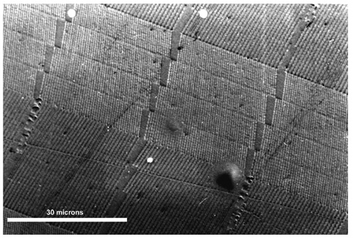
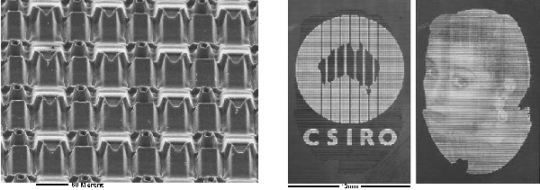
While the Catpix optical security microstructure provided a solution to the problem of crumpled banknote surfaces, it was very limited in the type of input artwork or graphics that could be converted into optically variable form, and this very much limited its industrial usability. The Captain Cook Catpix image on the 1988 polymer banknote, for example, shows a very stylised portrait of Captain Cook. In no way could the Catpix technology be used to represent graphical images of arbitrary form – and yet this was what was specifically required by banknote printers – as expressed explicitly by the Reserve Bank of Australia and the Bank of England Printing Works. In particular security printers like to use intaglio printed human portraits on their banknotes; the main reason being that portraits are easily recognisable by the public and therefore any errors in the portrait (e.g. due to attempted forgery) can be quickly identified and reported by the public. To solve the problem of converting any optically invariable graphical image into optically variable form a new OVD technology was required. This was the Pixelgram technology developed in the CSIRO Division of Materials Science and Technology during the period 1989-1993. Pixelgram solved this problem by regarding any optically invariable graphical image as consisting of a collection of independent pixels of various colours and intensity values, and replacing each pixel by a miniature diffraction grating with (i) the spacing between the grating grooves representing the colour of the pixel and (ii) the curvature of the grating rulings representing the colour intensity parameter of the pixel. Since a typical image might consist of 1000 x 1000 pixels this meant that the OVD version of the image would consist of 1 million miniature, generalised, curvilinear, diffraction gratings, with each grating consisting of 1000 x 1000 addressable points through which the grating rulings needed to be defined.
A typical Pixelgram OVD was therefore defined by over one trillion precisely defined exposure points – each exposure point being approximately 30 nanometres in diameter. A typical Pixelgram OVD would consist of 3-4 billion miniature polygons precisely positioned within a square inch area. Between 1988 and 1989 the mathematics and optical physics of Pixelgram was worked out and a general software package developed which could produce Pixelgram data files for any input graphical image. The software incorporated a pixel palette feature which reduced the image to a fixed number of colours and colour intensities in order to make the data handling more managable. The problem now was how to make such a device. No holographic or optical process could be used because the resolution of such devices is limited at the very best to the wavelength of the light used. Even 300nm UV light was 10X larger than the feature size required. The obvious answer was to use the ultra high resolution process of electron beam lithography.
The problem was could ebeam lithography write the huge file sizes required, and if so, could it do so within a reasonable timeframe. Two of the world’s premier electron beam lithography companies were approached with this question – JEOL of Japan and the Cambridge Instruments company of the UK. After the supply of test files under confidentiality agreement the answer was not long in coming from JEOL – “…. There is not enough disk space in the whole of Japan to do what you want to doâ€. The Cambridge group on the other hand regarded the problem as a challenge to their software and engineering skills and over the following two years produced a set of modifications to their EBMF 10.5 Ebeam system to allow the job to be done. These changes included hardware modifications to the pattern generator, machine software modifications, the development of an application specific software package, the fitting of an intelligent disk system for faster data transfer to the pattern generator, controlling the electron beam current stability to one part in 107 and controlling the external temperature environment to with 0.1 of a degree. The end result was an ebeam that could write 8X faster than a standard machine and routinely produce a Pixelgram master plate within 24 hours. Many of these machine modifications are now standard on ebeam systems, however in 1989 it was all very new and untried. It can therefore truly be said that the Pixelgram project also drove the development of ebeam technology into new directions and new application areas. From1992 onwards Pixelgram became a fully commercially competitive product able to produce a large range of easily recognisable high security optical effects, unmatched even by the Swiss Kinegram technology – the leading OVD technology at the time. A small section of a Pixelgram OVD is shown in the optical micrograph below.
Exelgram®
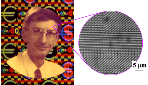
Pixelgram OVD technology provided a complete toolkit for the origination of a wide range of optical effects from optically variable portraiture – where the image switched from a positive to negative tone as the angle of view changed, to multichannel effects – where the image switched from one type of graphic to a totally different type of graphic, to moving kinematic effects, diffractive microtext, right angle effects, etc. Pixelgram was also a continuously upgradable technology where new optical effects could be easily incorporated in response to customer demand. What did not change however was the fundamental microstructure architecture, which consisted of a very large array of individual generalised diffraction grating pixels – each with very clear pixel boundary. This was not a problem initially, however as the demand for increased picture resolution increased, and therefore the size of the grating pixels reduced, a problem arose from the increased diffuse optical scattering from these pixel boundaries. This diffuse scattering subtracted from the amount of light available for diffraction and consequently reduced the overall brightness of the OVD image. In 1993 this problem was solved by the development of Exelgram technology, which was also developed within the CSIRO Division of Materials Science and Technology. Exelgram technology solved the diffuse scattering problem by replacing individual pixels by tracks or strips of continuously connected grating regions, thus removing diffuse scattering effects from either the x or y axis of the microstructure architecture. Exelgram reproduced all the optical effects available from Pixelgram with the added benefit of improved image brightness and fidelity. Exelgram used different diffraction grating pixel palette structures to Pixelgram, but exactly the same ebeam origination process. All of CSIRO’s commercial OVD projects were delivered using Exelgram technology.
Related OVD technology developments
During the period 1993-2000 the CSIRO OVD group operating out of the Division of Materials Science and Technology devoted most of its time to delivering on commercial projects and supporting the activities of CSIRO’s Exelgram licensees in Europe and the US. Most of this activity involved the production of Exelgram master plates originated by the high security electron beam lithography laboratory operated by the OVD group within the Division. In the time remaining outside of these commercial activities a significant amount of effort was also devoted to researching new OVD effects in response to perceived future market demand. These new patented OVD products included:
- the Vectorgram and OSM5 alternative OVD microstructures to Exelgram;
- an optical data storage technology based on a Pixelgram Optical Pulse Sampling (POPS) mechanism,
- a new optically variable ink technology based on the use of diffractive foil flakes,
- a micrographics effect patent and a biometric OVD technology capable of personalisation and specifically designed for identity document applications.
Commercialisation in a highly competitive environment
Commercialisation of the various CSIRO OVD technologies was an “interesting†process. Catpix was relatively straightforward. The Catpix patent application was sold to the Reserve Bank of Australia (RBA) as part of the polymer banknote technology package – bringing significant income to CSIRO. After Pixelgram was developed, and given that it was a dramatically better technology than Catpix, it was natural for CSIRO to also offer it to the RBA. However after several attempts to interest the RBA in the technology the bank declined. CSIRO then presented the technology at several US and European anti-counterfeiting conferences, where early samples of the technology were also displayed. As a result of this disclosure there was considerable interest in Pixelgram, with some high-end European security print groups willing to pay a very high royalty for a license to produce Pixelgram hot stamping foils. As a result, in 1991/92 license agreements were put in place with several high end security foil manufacturers in Europe. These licensees were responsible for both the global marketing of the technology and the manufacture of Pixelgram foils for various commercial projects. Later, in1994, these license arrangements were extended to the new Exelgram technology, which ultimately resulted in CSIRO securing several key projects in Europe and the US, thereby cementing Exelgram as a proven industrial application.
The securing of these projects was not easy, as the established industry groups fought extremely hard to keep this new OVD entrant out of their market patch. The credit for overcoming these difficulties is largely due to CSIRO’s OVD commercial group under the leadership of the Chief of Division Dr Mike Murray with strong legal support provided by CSIRO’s legal group under Mr Terry Healy. Without these efforts, particularly in regard to the extremely aggressive Amex competition, it is unlikely that Exelgram would have survived, leaving the many millions of dollars of commercial income (royalties, license fees and plate sales) generated by the technology unrealised. An interesting aspect of Exelgram’s marketplace influence during this period can be found in the effect the technology had on its OVD competition. At the time all of the competing OVD technologies, including the Swiss Kinegram technology, were based on optical lithography origination processes of one type or another. Ultimately the high security optical effects advantages offered by electron beam lithography, which had been clearly demonstrated by Exelgram, were too compelling for the competition to resist. Today electron beam lithography has become the standard method used by the major US and European security print groups for originating high security OVDs for banknotes and Government issued identity documents.
Optically Variable Intaglio Device (OVID), a response to counterfeiter’s increasing sophistication
While Exelgram certainly achieved all of its technical objectives and had well demonstrated its anti-counterfeiting capabilities via its performance on several commercial projects, it was clear by the end of the 1990’s that the counterfeiters had not been idle during this time. In response to the new banknote OVD technologies counterfeiters had become much better organised, with some groups – particularly those operating in Eastern Europe, adopting rogue company structures; board meetings of the company determining via a risk/reward or strength-weakness-opportunity- threat (SWOT) strategy which particular currency and banknote to counterfeit at any particular time. These groups also acquired through normal commercial channels dot matrix holographic systems, electroplating and recombination equipment and associated foil technology to allow them to mass produce OVD foils to incorporate into their counterfeit banknotes. The figure below shows a high quality counterfeit Euro banknote produced by this process.
Although these dot matrix-originated counterfeit OVDs do not display the same high security optical effects as the original and can easily be detected as forgeries under close examination, they are sometimes sufficiently close in their optical brightness and movement effects to fool the public. In this regard the counterfeiters are exploiting a key weakness associated with all banknote security features; the very limited timeframe (normally two to five seconds), that the public user of banknotes allocates to the authentication process in their daily financial transactions. An effective anti-counterfeiting feature must be able to be authenticated extremely quickly and naturally by the public. Since most, if not all, diffractive OVD technologies have some difficulty fulfilling this requirement it was decided in 2000 to look at a new approach to this OVD problem. The desire to take a fresh look at the OVD problem was also stimulated by a further consideration of a commercial nature. Up until that time all the OVD technologies being offered to the security printing industry were of the diffractive type with grating groove depths of the order of 0.5 micron or less. Such shallow microstructure depths required that the microstructure be first embossed into a thin foil substrate. This foil was then hot stamped onto the banknote substrate. Even the Captain Cook Catpix OVD had to be stamped onto the polymer substrate via this intermediate foil process. From a commercial perspective this meant that a lot of the commercial return from an OVD project went into the pockets of the foil manufacturers.
From CSIRO’s perspective it would be highly advantageous if the foil phase of the process could be eliminated so that more value could be put into the optical microstructure. The OVD technology developed to solve this commercial problem as well as the problem of differentiation from diffractive devices was called the optically variable intaglio device (OVID). OVID was developed in the CSIRO Division of Manufacturing Science and Technology from the year 2000 onwards. Instead of a diffractive microstructure, OVID used a micromirror architecture – originated via a combination of electron beam lithography and photolithography. Because the micromirror depths ranged from 15 – 30 microns – in contrast to the 0.5 micron depths of diffractive devices, OVID could be directly printed onto the banknote substrate without the need for foil. OVID also produced white light image effects over wide angles of view. These effects were therefore highly differentiable from the rainbow like narrow bandwidth effects of diffractive devices. The surface of the OVID image also generated a ‘roughness’ or ‘intaglio effect’ due to the depth of the micromirror array, and so could be authenticated by feel as well as by sight. Finally OVID could also be incorporated into the clear windows of polymer banknotes to provide an optically variable watermark effect. In this mode of operation, the micromirrors defining sub-structure of the device acted like microprisms.
Final comments
OVID was the last of the key developments which defined the work of the CSIRO OVD group. The closure of the project in 2006 after twenty years of research and commercialisation brought to an end a unique episode in the history of the organization. While the income from the various commercial projects during this period amounted to almost ten million dollars, the more important benefit has been the impact the project has had on the security printing industry in terms of both direct and indirect influences. The direct benefits can be measured by both the preservation of the integrity of the security documents which incorporated Exelgram foils and the cost savings associated with these protections. For example, prior to the adoption of Exelgram, American Express were losing up to US$100,000 per day through the counterfeiting of their Travellers cheques. Another direct influence – this time in an Australian context, was in the development of a set of document security protocols for new Australian identity documents. The OVD project’s indirect influences were largely related to demonstrating the value of pixel based electron beam lithography OVD origination over the various types of holographic origination. These holographic type approaches are now not regarded as an effective approach to high security OVD origination. OVID has also had an influence on the market. In the past two years (2011-12) competitors to this technology have started to appear. These competing micro-mirror and micro-prism array devices, together with other types of OVD technologies currently being developed by various security printing groups will hopefully continue to help the industry to stay one step ahead of the counterfeiters.
Finally, it would be less than honest to finish this story without at least mentioning in passing the sorry tale of litigation that was associated with the OVD project for a major part of its history. The cost of this litigation was not just large in a financial sense, but also large in terms of lost project opportunities and related income streams. However, for ongoing confidentiality reasons, this story must remain untold. Confidentiality clauses are often used to protect particular groups from scrutiny, and this case is no exception.
People
The success of the CSIRO OVD group in developing a range of technologies which challenged the established industry offerings and ultimately caused that industry to change direction is largely due to the quality and dedication of its staff. These staff members and their main project activities and time of involvement are listed below. Some of the staff listed below were associated with the project on a part time basis during their years of involvement while others were full time.
|
Dr Tim Davis: |
OVID Photolithography (2003-2005). Part time. |
|
Mr David Gough: |
Machine reader system for Pixelgram Optical Pulse Sampling (POPS) technology. Part time. |
|
Mr Terry Healy: |
Legal support (1991-2000). Part time. |
|
Dr Zoltan Hegedus: |
Grating theory and counterfeit resistance testing of Exelgram -(1995 – 1998). Part time. |
|
Dr Tien Kieu: |
Artwork development, OVD palette development. (1997- 2000). |
|
Dr Robert Lee: |
OVD project leader, Generalised grating theory development, inventor of the Catpix, Pixelgram, Exelgram |
|
Dr Patrick Leech: |
OVID Photolithography and artwork development (2000-2006) |
|
Dr Victor Maslen: |
Software development and artwork development. (1993 -2000) |
|
Mr Russell Marnock: |
Electron beam lithography. (1995-2005) |
|
Dr Mike Murray: |
Chief of Division and OVD commercialisation leadership. – (1987 – 1997). Part time. |
|
Mr John Patterson: |
Electron beam lithography. (1993-1998). Part time. |
|
Mr Grahame Quint: |
Ebeam lithography software development, OVD palette development. (1989-1998) |
|
Mr Selwyn Glanville: |
Optical and scanning electron microscope characterisation – (1994 – 1996). Part time. |
|
Dr Brett Sexton: |
Precision electroplating and AFM characterisation – (1998-2005). Part time. |
|
Ms Fiona Smith: |
Precision electroplating (1998-2005) . Part time. |
|
Mr Greg Smith: |
Commercialisation. (1991-1995). Part time. |
|
Dr Xiaoping Yang: |
OVD microstructure palette development and artwork design. (1995- 1999). Part time. |
As well as the above CSIRO contributions, it is important to mention that there were several local and international companies that provided significant contributions in the early stages of the project. These companies provided their support free of charge and – particularly in the case of Pixelgram, the technology would not have got off the ground without this critical early support. These companies and their contributions are listed below.
|
Cambridge Instruments (UK) – now Vistec |
Electron beam lithography – (1989-1991) |
|
Leonhard Kurz group (Germany) |
Hot stamping foil technology – (1989-1991) |
|
Astor Universal (UK) |
Hot stamping foil technology. – (1990 – 1991) |
|
Disctronics (Australia) |
Precision electroplating – (1989 – 1991) |
|
Leigh Mardon (Australia) |
Plastic cards and printing – (1989-1990) |
Source
Lee RA, 2013, personal communication.
Related Information
A more detailed review of CSIRO’s OVD developments can be found in Chapter 7 of “Micromanufacturing and Nanotechnologyâ€, (Mahalik NP, ed), Springer-Verlag Berlin Heidelberg 2006. ISBN-10 3-540-25377-7 and ISBN-13 978-3-540-25377-8
A century of innovation – EXELGRAM anti-counterfeiting technology – Powerhouse Museum
Parliament of Australia, House of Representatives, “Grievance Debate – Catpix and Pixelgram Technology†Hansard, 17-12-1992, Parl. No. 36, Page 4037, System ID: chamber/hansardr/1992-12-17/0080.
Parliament of Australia, House of Representatives, Questions on Notice, “Pixelgram and Exelgram Technologiesâ€,Question 2574, Wednesday, 4 March 1998.